An all-electrical detection of plasmons propagating in a graphene waveguide
All-electrical plasmon detector. Plasmons are charge density waves of nearly-free electrons that occur in conductors like metals or doped semiconductors and oscillate in space and time. These oscillations are sustained by the Coulomb force generated by charge inhomogeneities and can couple strongly to electromagnetic fields.
Recent years witnessed a renewed interest in surface plasmons (plasmons that are confined to the surface of a conductor) and plasmons in the recently discovered two-dimensional materials (mono and few-layer graphene, transition metal dichalcogenides...) and their heterostructures.
Two-dimensional plasmons offer an efficient way to confine and guide light on distances smaller than its free-space wavelength and can be useful in many optoelectronic devices such as photodetectors working in various regions of the electromagnetic spectrum, with applications ranging from bio-imaging to telecommunications. The key ingredients of an effective plasmonic technology are the abilities to launch, guide, manipulate and detect plasmons in a device.
Our device aims to solve the last of these problems, paving the way for an all-electrical detection of plasmons propagating in a graphene waveguide.
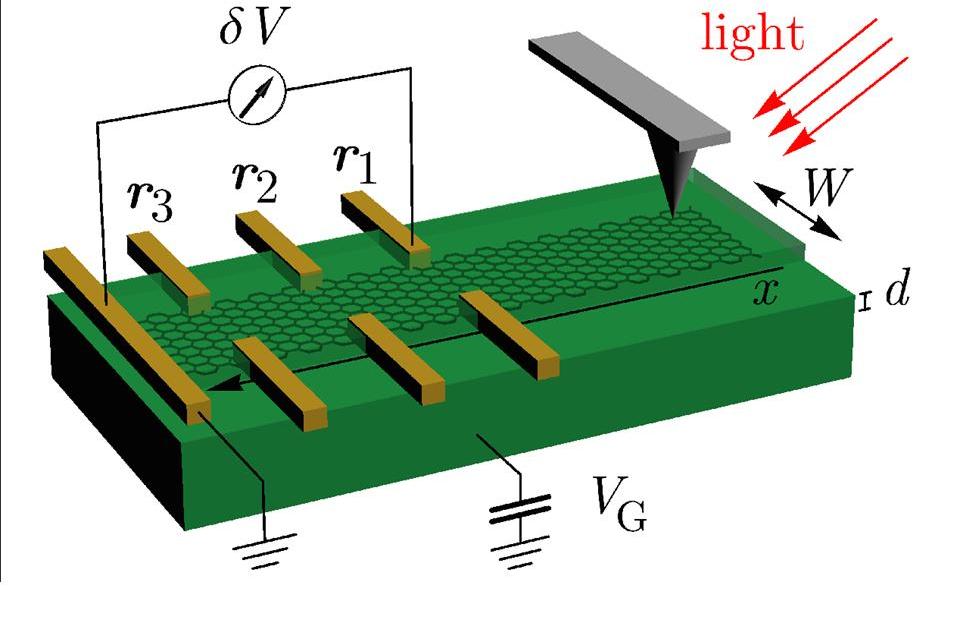
It is composed of a graphene waveguide with electrical contacts placed on its side. When a plasmon is launched at one end of the waveguide a potential difference builds up between the lateral contacts and a reference contact placed at the end of the waveguide. Measuring this potential difference enables the detection of plasmons propagating in the waveguide. Our detection scheme relies on the non-linearities in the response of graphene electrons to a perturbation and does not require the coupling of the waveguide to an external detector.
This allows a simpler on-chip implementation and implies the absence of a low-frequency cut-off due to the energy gap of semiconductor detectors that are important advantages with respect to present-day technologies.
See more at: Iacopo Torre, Andrea Tomadin, Roman Krahne, Vittorio Pellegrini, and Marco Polini, Electrical plasmon detection in graphene waveguides, Phys. Rev. B 91, 081402(R) – Published 5 February 2015, link: http://journals.aps.org/prb/abstract/10.1103/PhysRevB.91.081402
Schematics of our electrical plasmon detector. A graphene strip of width W is encapsulated between two dielectrics. A back gate (dark blue slab), separated by a distance d from the graphene sheet and held at a voltage VG, is used to control the average carrier density in graphene. At one end of the strip, a plasmon is launched by using, e.g. a metallized atomic force microscope tip illuminated by light. Due to non-linearities in graphene response, a dc electrical potential difference δV is measured between probe electrodes placed at positions r1, r2, and r3 and a reference electrode placed at the other end of the strip. The quantity δV provides a direct measurement of the ac electric field of a propagating plasmon.


